Samsung Proposes Way to Compensate the Local Black Level Variations

...
Samsung patent application US20140014818 "Pixel array, image sensor including the same, and method of compensating for local dark current" by Young Sung Cho, Dong Jae Lee, Tae Chan Kim, and Tomer Livneh propose a simple approach to compensate the black level variations across the pixel array. The idea is simple: a number of dark, light-shielded pixels is distributed in random or not-so-random way across the array, and their interpolated output is used for local black level calculations:


There are few modifications that need to be added to that application:

  • Light leaks or photoelectrons diffusion to the shielded pixels can distort the black level measurements. Unless this is completely resolved in the company's ISOCELL technology, one might need to light-block the larger groups of pixels.
  • dark current varies a lot on pixel-by-pixel basis. So, it needs to be somehow averaged across the neighboring dark pixels
  • there are hot pixels, whose dark current is just abnormally high and carries no information about other pixels in the area. They need to be excluded from the dark current calculation process.
5:51 AM

Sony Proposes Column-Parallel ADC Crosstalk Reduction Approach

...
Sony patent application US20140022430 "Solid-state imaging device and manufacturing method" by Yosuke Ueno, Natsuko Seino, and Kenichi Takamiya discusses a crosstalk challenge between the adjacent column-parallel ramp ADCs. As pixel size shrinks, the column pitch becomes smaller, the neighboring comparator's transistors are closer and coupling capacitance becomes more of the issue. One possible solution is to add metal shields between columns. However, the shield takes a significant column area. So, Sony proposes to re-arrange the comparator transistors in the neighboring columns in such a way that part of the crosstalk is compensated:

Column Ramp ADC (background info, nothing new)
Column comparator input stage (background info, nothing new)
The capacitive coupling problem shown (background info, nothing new)
Coupling caps from the above shown in schematics (nothing new so far)
One of the improvement proposals, coupling is partially compensated
Schamatics of the compensated layout,
Note that each half-nmos gets couping to the opposite side
of the neighboring diff pair
4:27 AM

Point Grey Cameras Comparison

...
Point Grey releases the charts comparing its different cameras based on CCD and global and rolling shutter sensors. Few interesting charts comparing monochrome sensors (see color sensors in another doc):


Thanks to MJ for the info!
11:32 AM

Cypress Offers Single-Chip MIPI-to-USB Bridge

...
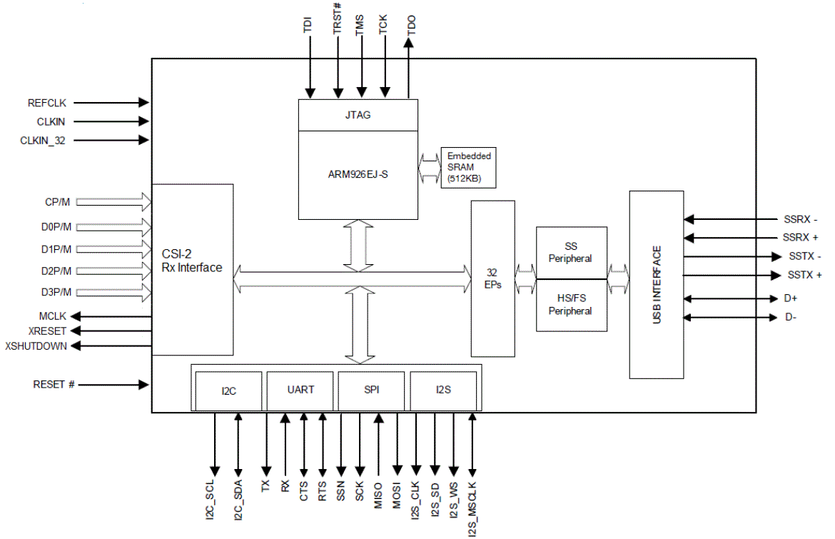
Cypress EZ-USB CX3 camera controller allows simple mobile image sensors connection to PC. CX3 has a 4-lane CSI-2 receiver with up to 1 Gbps on each lane, and supports video data formats such as RAW8/10/12/14, YUV422 (CCIR/ITU 8/10-bit), RGB888/666/565 and User-Defined 8-bit. CX3 has integrated the USB 3.0 and USB 2.0 PHYs along with a 32-bit ARM926EJ-S microprocessor for data processing and for building custom applications.

10:46 AM

DETECTION AND SEGMENTATION OF NORMAL AND PATHOLOGICAL TISSUES IN BRAIN MRI

...

ABSTRACT


 Segmentation of anatomical regions of the brain is the fundamental problem in medical image analysis. In this paper, a brain tumor segmentation method has been developed and validated segmentation on 2D MRI Data. This method can segment a tumor provided that the desired parameters are set properly. This method does not require any initialization while the others require an initialization inside the tumor. In our segmentation approach adaptive boost segmentation algorithm is used. it uses the intensity as a parameter to segment the whole image data set. The input MRI image is preprocessed and loaded into matlab workspace. In the segmentation process the image is divided into blocks depending on the edge, gray and threshold parameter. The blocks are divided by comparing the intensity value of the image with the parameters as the intensity of the tumor affected area will be higher. Likewise the tumor surface from the MRI image is segmented out. After the detection of the tumor it is then classified using adaptiveboost algorithm which gives the type of the tumor for the doctor's convenience. Here the threshold limit is applied to each image and the limit is tested on the adaptiveboost  algorithm.


Key words- AdaBoost classifier, brain Tumor Detection, Segmentation,  Fractal, MRI, Multi-FractalAnalysis,  MultiresolutionWavelet, Texture Modeling.

need this project contact us


8k Video in Endoscope Form Factor

...
Tech-On reports that Shinko Optical Co was able to make an endoscope based on Hitachi Kokusai Electric 8K video camera (8K x 4K resolution). Tech-On thinks that 8k video might be widely adopted in the medical industry earlier than in the TV broadcasting. The more detailed video is said to eliminate the need in surgical loupes and maintains the details from farther distance. No info is given on the 8k sensor size or its pixel size.
1:17 PM

Sony Buys 12-inch Renesas Fab to Expand Image Sensor Production

...
Sony announces the acquisition of Renesas Tsuruoka Fab. Once the transaction is closed on March 31, 2014, Sony will establish Sony Yamagata Technology Center ("Yamagata TEC").

Last year, there were media reports that Renesas is going to close its Tsuruoka fab. The fab used to make chips for Nintendo game console, whose sales were sluggish.

Yamagata TEC will serve as a new production site for CMOS image sensors, and Sony plans to engage in capital investment from the first half of the fiscal year ending March 31, 2015 ("FY14") through the second half of the fiscal year ending March 31, 2016 ("FY15") in order to increase image sensor production capacity. This planned investment is a part of Sony's mid- to long-term plan to increase its total production capacity for image sensors from the current capacity of approximately 60,000 wafers per month to approximately 75,000 wafers per month (in 300mm wafer equivalents). Sony intends to convert part of the semiconductor manufacturing equipment that Sony is scheduled to acquire from Renesas to CMOS image sensor manufacturing, and also to install new equipment for CMOS image sensors. Yamagata TEC will primarily engage in the manufacture of photodiodes and wiring processes for stacked CMOS image sensors.

Sony will position Yamagata TEC as a new site for one phase of the image sensor wafer production process, alongside its existing Kagoshima Technology Center, Kumamoto Technology Center, and Nagasaki Technology Center sites. By doing so, Sony aims to strengthen its capacity to supply stacked CMOS image sensors.

The total investment amount is expected to be approximately 35 billion yen, comprising (i) approximately 7.5 billion yen to acquire Renesas Yamagata Semiconductor's Tsuruoka Factory assets in the fiscal year ending March 31, 2014 ("FY13"), and (ii) approximately 27.5 billion yen for planned capital investment to be carried out during FY14-FY15.

Update: Semicon portal published a nice graphics on the recent Japanese fabs acquisitions. The portal also says that Tsuruoka fab has 40nm process, a nice advance for Sony. There are some challenges for Sony in this deal:

"Renesas moved some of the production equipment to the Naka fab, its main fab, so that it could continue manufacturing game-use system-on-chip LSIs, the Tsuruoka fab's principal products. Sony, therefore, would have to install some production equipment following the contemplated acquisition. This would increase the aggregate investment related to the Tsuruoka fab. Opinion on the advisability of the acquisition is divided within Sony.

From Sony's perspective, another drawback of the Tsuruoka fab is that the production line is not fully automated. Originally designed for high-mix low-volume production, the fab has poor automatic conveyor systems. Therefore, the line could fall short of what is required for highly efficient high-volume manufacturing of CMOS image sensors by Sony.
"

Update #2: Sony publishes a map of its image sensor production facilities:

2:28 AM

Senior Piping Stress Engineer - Aker Solutions

...


Senior Piping Stress Engineer - Aker Solutions
Location: Aberdeen
Position type: Contract Department: 803 Talisman Flyndre (125)

Corporate overview:

Aker Solutions provides oilfield products, systems and services for customers in the oil and gas industry world-wide. The company's knowledge and technologies span from reservoir to production and through the life of a field. Aker Solutions

Senior Piping Designer Vacancy available in Finland

...


Dear Candidates,


Our client Enersense International
are urgently recruiting for a Senior Piping Designer to work in Pori,
Finland:


Job
Title:             Senior Piping Designer

Location:            
Pori, Finland

Salary:                 
Negotiable

Job
Type:             Permanent


The Designer will be responsible for preparing layout and design the
complex underwater transmission

Piping & Layout - Senior Engineer Norway

...


Piping & Layout - Senior Engineer

 Rosenberg WorleyParsons AS The department’s job consists of designing piping and pipe support including create 3D models, perform stress calculations and prepare requisitions for piping and pipe support materials. We have the technical responsibility for manual valves in our projects. We establish and maintain the required specifications in PDMS for 3D

Samsung ISOCELL Technology Webinar

...
IEEE Tech Insider opens registration for a free Samsung webinar on Feb 11, 2014: "Image Sensors for Mobile Devices: Next Generation Pixel Technology" by Jungchak Ahn, VP of Samsung Electronics’ Image Sensor Product Development, and Marty Agan, Director Engineering in the System LSI business of Samsung Semiconductor.

Samsung presenters will share with the audience how ISOCELL:
  • Decreases crosstalk by approximately 30%, resulting in higher color fidelity
  • Increases the full well capacity by 30%, leading to greater dynamic range
  • Features a 20% wider chief ray, reducing the height of the camera module
They also talk about specific challenges in developing ISOCELL and the solutions that will benefit camera module designs and, ultimately, the end camera applications.
12:31 PM

Under the Cloud

...

The business world is almost as fad-ridden as the education world, and one of the hot words in the last few years is "cloud" as in "I'll get it from the cloud," or "We put all our data on the cloud."  In this sense, the word means a set of Internet servers where your important data is archived so that it is accessible from anywhere that has an Internet connection.  The concept is increasingly vital to commercial and institutional users worldwide, and makes sense in that context.  But as Scientific American columnist David Pogue warns in the February issue, Apple and Microsoft are taking not-so-subtle steps to force many individual users of their products onto the cloud.  And I doubt that anyone reading this column can avoid using Apple and Microsoft products without a lot of inconvenience. 

The situation, as I understand it, is basically this:  suppose you have data that needs continual updating on your portable gizmo (which can be an iPad, an iPhone, a BlackBerry, one of those Android things, or you name it), and you'd also like the same version of the same data on your laptop.  In the old days, whenever you made changes on your calendar, for example, you would then physically plug your portable device through a USB cable or whatnot into your laptop and tell it to sync.  That way, your laptop calendar would agree with your handheld thingy's calendar and vice versa, and you wouldn't find yourself at Aunt Mimi's when you were supposed to be having your teeth cleaned.  So far, so good.

Then the number of handheld devices proliferated, and so did their operating systems, and so did the ways you can have laptops and towers talk with portable systems (wireless, IR, Bluetooth, etc.), and at least according to the manufacturers and their unofficial representatives, it just got to be too hard to come up with proprietary software to sync absolutely every portable thingamajig with each operating system for all the popular computers.  So they just said forget it:  the real data will sit on the cloud, where we can keep track of it, and then all we have to do is make sure that every piece of hardware (portable or not) can keep in touch with the cloud.  And that solved the problem. . . .

But if you were used to firing up your old laptop and plugging it into your BlackBerry that you've had since 2003, and you are dead-set against keeping your data in a place that you know not where and you know not when it might go down, you are now out in the cold and under the cloud, so to speak.  According to Mr. Pogue, the latest operating systems from both Apple and Microsoft either don't allow you to do hard-wired transfers without involving the cloud, or make it so hard to do that you almost have to get a networking certificate from Microsoft to know how to do it. A discussion thread on an Apple forum on exactly this topic has been going on since last October, and has accumulated 150 pages of comments.  So there are more than a few people upset about this.

Call me Amish, but it doesn't affect me because my form of a BlackBerry is a three-by-five card.  Or rather, many three-by-five cards.  I suppose if you took all the three-by-five cards I've used in the last decade and piled them up, they would make a stack high enough to fall over and form the kind of mess my desk looks like some days.  In fact, that may be why. . . anyway, somehow I have survived thirty years of an occasionally intense professional life with nothing more advanced than a laptop or two and a mobile phone that you still have to use the numeric keypad for to send a text.  It's so annoying to do it that way that I hardly ever send texts, which is all right by me. 

But seriously, this specific issue is an example of a more general trend that organizations are following: a move toward exerting increasing control of any computer that is connected to one of their networks.  For example, I spend some time at the University of Texas at Austin.  If I was using a University-provided laptop (which I'm not, as it turns out), I would now have to make sure that all the data on it was encrypted in accordance with a University-provided type of encryption software so that if it happens to get stolen, the thieves can't run off with University data.  That makes sense from a liability and security point of view—I have blogged on numerous scandals and crimes that happened when someone took home a laptop full of supposedly secure data—but it represents another intrusion, if you will, into a space that was formerly rather private. 

Of course, if the University owns the laptop, they get to say what you can and can't do with it.  Privately owned computers connected to privately rented networks are another matter, but then you still have to deal with Apple or Microsoft, and their pressure to keep your stuff on the cloud will prove irresistible.  The Star Trek Borg, a race of cybernetic beings, liked to say "resistance is futile," but that was only a TV show.   

Personally, I don't see any real harm in letting Microsoft know the details of my next dental appointment.  And yes, those massive servers go down from time to time, but then so does your laptop.  I admit that I would feel a certain kind of existential queasiness in entrusting the only record of my professional schedule to some ethereal system that is everywhere and nowhere, rather than having it in a tangible, solid form on pieces of paper in my appointment calendar in my briefcase.  (Yes, I do that the old-fashioned way too.)  Maybe people living in the 1850s felt the same way about the newfangled electromagnetic telegrams, and didn't really trust them on an instinctive level as much as they would trust a letter written by the hand of a friend they knew.  But they got used to trusting telegrams, and I suppose we will get used to trusting the cloud, as long as our trust is not abused. 

Sources:  The online version of David Pogue's article "The Curse of the Cloud" can be found at http://www.scientificamerican.com/article/were-forced-to-use-cloud-services-but-at-what-cost/.  I also referred to Wikipedia articles on BlackBerry and Borg (Star Trek). 

Pipe Flanges – Do’s and Don’ts

...


Pipe Flanges – DO’s and DON’Ts


 DOs:


a) Always visually inspect the surface finish of the flange
for injurious defects. It should be clean, degreased and free of any defects,
nicks or burrs. The permissible imperfections in flange surface finish
specified in ASME B16.5, Table 3 are not allowed for critical applications.
Raised Face and Flat Face flanges should also be checked for

Lead /Senior Piping Designers - Qatar WorleyParsons

...


Lead /Senior Piping Designers 
Job Type Full-time Advertising Category Engineering/Design & Sciences Location of Job Doha, QA (Primary)
Doha, DW 18130 QA
Job Description •Produce the various piping deliverables to the agreed schedule.

•Apply recognised offshore / onshore engineering practices applicable to piping design and topside/plant layout.

•Apply good interpersonal skills, liaising with

Geo Semi Introduces Single-Chip Wide Angle HDR Camera Processor

...
GEO Semiconductor introduces the GC6500 family of programmable video processors, integrating GEO’s eWARP core, Apical HDR ISP pipeline, MIPI D-PHY Input, stereo recording path, H.264 Codec, Tensilica XTENSA HIFI CPU and USB2.0 interfaces. Integrated DCDC converters and LDOs provide all necessary system voltages. The eWARP Geometric Processor supports correction for wide field of view lens (180/360). It also supports custom maps for panoramic and zero-content loss views, multiple virtual cameras with perspective correction and ePTZ (electronic Pan, Tilt and Zoom). The processor supports up to 5MP sensor resolution at 30fps and 1080p60 video.

Paul Russo, CEO of GEO Semiconductor says, "There is an explosion of uses for ultra-wide field of view or ‘fisheye’ applications for consumer and industrial markets, such as home security, automotive, cloud and wearable cameras. All of these segments require intense geometric image processing as well as multi-stream compression support. The programmability of the GC6500 provides customers ultimate flexibility and offers H.264 video compression, WDR ISP support in a highly integrated low power IC to enable emerging camera markets. GEO has developed complete software stacks, including iOS and Android applications, to provide superior hardware and software support to its customers and shorten their time to market."

10:31 PM

Eric Fossum Presents CMOS Sensor History in Fermilab

...
Fermilab publishes Eric Fossum's presentation "CMOS Image Sensors: Tech Transfer from Saturn to your Cell Phone", including an interesting Q&A section in the end, presented on Nov 18, 2013 (via Nuit Blanche blog):


10:05 AM

Phase One Features Medium Format Sony Sensor

...
Cnet, Luminous Landscape, Digital Transitions report that the new Phase One IQ250 medium format digital camera back features 50MP Sony CMOS sensor. The sensor size is 44mm x 33mm (1.3x MF crop factor)and it offers 14-stops DR.

Luminous Landscape also says that the Hasselblad H5D-50C uses the same Sony sensor.

Phase One's Youtube video talks about the new CMOS sensor:

1:47 PM

Brigates Announces MCCD Sensors for Security Cameras

...
Brigates (Chinese name - Rui Kunshan Microelectronics Inc.) announces BG0601 and BG0631 MCCD sensors for PAL-resolution security cameras. MCCD is a CMOS sensor which has CCD-compatible external interface. It be used in place of CCD in security camera, with some modifications: AFE is integrated onto the sensor and HV driver is not needed:

Brigates Chairman Luo Wenzhe presents MCCD technology
9:15 AM

e2v on Gaia Sensor

...
e2v published a PR on its 106 CCDs imager inside the European Space Agency space observatory Gaia on a five year mission to map the galaxy. e2v has implemented different functionalities in each of these CCDs, like charge injection, antiblooming and TDI gate structures to meet the specific needs of the mission. There are three variants of the CCD91-72, each optimised for different wavelengths in the range 250 to 1,000nm. The CCD package is 3 sided buttable, to minimise the dead space between CCDs when they are tiled together in the mosaic and all CCDs have been through e2v’s back thinning process.

Hans Faulks, General Business Unit Manager for Space and Astronomy commented: "We are immensely proud and excited to finally see our image sensors embark on this mission. All the hard work, dedication and expertise that has been put into our sensors and into the mission will finally come to fruition. Our products will now play their part in history as we help increase our understanding of our universe."

4:53 AM

Pelican Imaging News

...
Pelican Imaging started the new year with quite a few news. First, its website is updated with special emphasis on depth-enabled features:


Second, the company publishes its CTO and co-founder Kartik Venkataraman's keynote on the future of mobile imaging presented at the International Conference on Consumer Electronics (ICCE) on January 12 in Las Vegas, NV. The keynote addresses some of the concerns about the array camera resolution (click to enlarge):


The presentation also talks about the depth-enabled features, after-the-fact focus, background blurring and substitution, videoconferencing, and more. The depth map is not bad for such a small camera:


Third news is that Pelican Imaging's technology has been nominated for a 2014 Edison Award - the nominee #181 out of 309. The winners will be announced on April 30.
11:15 AM

New Imaging Technology Unveils Two New WDR Products

...
New Imaging Technology (NIT) presents its WDR Intensified modules, the first intensified Night Vision cameras with a WDR of more than 140dB. The new WiDy IntenS cameras feature a low power consumption (< 300 mW for the analog version) and a small form factor.


NIT also introduces a new WDR InGaAs products family, including sensors and camera modules. NIT SWIR products are based on a proprietary Wide Dynamic Range ROIC technologies and offer aDR of more than 140dB in a single image.
10:32 AM

EXPERIMENTAL INVESTIGATION ON CEMENT CONTAINING NANO PARTICLES

...

         Nanotechnology concerns materials and systems whose structure and components exhibit novel and significantly improved physical, chemical and biological properties, due to their nano scale size. Simply put, nanotechnology deals with particles ranging anywhere from 1 to 100 nm. Application of nano-materials into the production of cement and concrete can lead to improvements in civil infrastructure because the mechanical strength and life of concrete structures are determined by the micro-structure and by the mass transfer in nano-scale.

     Better understanding and precise engineering of an extremely complex structure of cement based materials at the nano level will apparently result in a new generation of concrete that is stronger and more durable with desired stress-strain behaviour and possibly possessing a range of newly introduced properties, such as electrical conductivity as well as temperature, moisture and stress-sensing abilities.

     Nano-particles are unique because their size affects the behavior of cement. A reduction in particle size can lead to a more rapid setting and hardening of cement due to stronger electrostatic attractive forces and a greater specific surface. Recent studies have shown that nano particles used as an additive to cement mortar can improve its mechanical properties. In recent century, very wide and effective research has seen on improving the properties of cement with incorporating wide range of supplementary cementing materials such as pozzolanas and nano particles due to increasing the use of cement from decade to decade.


NEED THIS PROJECT CONTACT US RS: 1000


Sent from Windows Mail

9:30 AM

INTELLIGENT ENERGY SAVING SYSTEM

...

Intelligent Energy Saving System can be used in places like where lighting is very important. The libraries will be well illuminated with many lamps. When people are not present at a reading place the lighting can be made OFF and when they are present, the lighting made ON. All these can be done through by Dimming circuit and PIR sensor.


            If a person entering to the monitored area, the PIR sensors activates and sense the person, gives to the micro controller. The Infrared energy emitted from the living body is focused by a Fresnel lens segment. Then only the PIR sensor activates. After sensing the person   LDR checks the light intensity of the monitored area, whether it is bright or dark. Depending on the LDR output, the lamp may be ON / OFF by using Dimmer circuit.


             By using this system we can adjust the speed of Fan according to the room temperature measured by Thermostat, which is connected to the micro controller.


            To display the room temperature of PIR mode operation we are using the LCD display.


9:17 AM

List of Railway Recruitment Control Board website address and email id , railway jobs

...