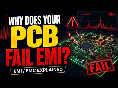
Electromagnetic Interference (EMI) and Electromagnetic Compatibility (EMC) compliance are among the most challenging hurdles in modern electronic hardware design. Failing an EMI/EMC test late in the product development cycle often leads to costly board spins, delayed product launches, and unexpected budget overruns. For hardware designers and modern Engineering IT professionals managing complex design ecosystems, understanding why printed circuit boards (PCBs) fail these crucial compliance tests is the first step toward building cleaner, more resilient products.
Common Root Causes of PCB EMI/EMC Test Failures
EMI issues generally occur when unwanted electromagnetic energy escapes a circuit board or when the system fails to withstand external radiation. The most frequent technical culprits include:
- Improper Grounding and Discontinuous Return Paths: When high-speed signal traces cross split ground planes, return currents are forced to take longer paths, creating large loop areas that act as active antennas emitting radiation.
- Poor Trace Routing and High-Speed Signals: Routing sensitive or high-frequency traces near the board edge or parallel to noisy lines increases cross-talk and severe differential-mode or common-mode emissions.
- Inadequate Power Delivery Network (PDN) Design: Inefficient placement of decoupling capacitors leads to power plane noise, ground bounce, and transient voltage spikes across high-speed ICs.
How Engineering IT Empowers Front-Loaded EMI Mitigation
Resolving electromagnetic issues can no longer rely on physical trial-and-error testing. Leading tech organizations rely on robust Engineering IT infrastructure to supply engineers with high-performance computing resources, streamlined Electronic Design Automation (EDA) toolchains, and 3D electromagnetic simulation software.
By integrating simulation tools directly into the initial design pipeline, engineering teams can perform virtual pre-compliance testing. Detecting board hot spots, analyzing signal integrity (SI/PI), and enforcing strict automated design rules prior to manufacturing ensures potential EMI hazards are rectified long before physical boards enter a certified test chamber.
Actionable Strategies for First-Pass EMC Compliance
To minimize compliance risks and optimize your hardware workflow, consider these fundamental design guidelines:
- Maintain Continuous Ground Planes: Keep reference planes uninterrupted beneath high-speed signals to minimize loop inductance.
- Optimize Board Layer Stackup: Position signal layers adjacent to continuous ground or power planes to provide immediate return paths.
- Incorporate Filtering at I/O Interfaces: Utilize ferrite beads, common-mode chokes, and proper connector shielding to prevent noise from propagating outside the enclosure.
- Standardize Workflows: Align your software environments using enterprise-grade Engineering IT solutions to ensure all team members adhere to standardized EMC rule sets during layout.
By adopting a proactive, simulation-first approach, engineering teams can significantly increase their EMI/EMC pass rates, lower manufacturing costs, and speed up market launch schedules.


